ISIR
The Institute of Scientific and Industrial Research, Osaka University
大阪大学
産業科学研究所
LAST UPDATE 2020/06/12
-
研究者氏名
Researcher Name陳伝彤 Chuantong CHEN
特任准教授 Specially Appointed Associate Professor -
所属
Professional Affiliation大阪大学産業科学研究所
フレキシブル3D実装協働研究所
The Institute of Scientific and Industrial Research, Osaka University
Laboratory of flexible and power three dimensional system integration -
研究キーワード
Research Keywordsパワーエレクトロニクス
実装技術
信頼性評価
鉛フリー技術
ナノテクノロジー
Power electronics
Packaging technology
Reliability evaluation
Pb-free technology
Nanotechnology
- 研究テーマ
Research Subject -
次世代パワー半導体実装材料と技術
Next-generation power semiconductor packaging materials and technologies
研究の背景 Background
パワー半導体は、電力変換ロスを大幅に低減し、高周波化により機器小型化を実現すると期待されている。このために生じるエネルギー密度上昇により200℃を超える動作が期待されるが、この厳しい環境における動作を保証する耐熱実装技術が欠如している。
Power semiconductors such as SiC,GaN are expected to significantly reduce power conversion loss and achieve device miniaturization due to its highly operation frequency, which can withstand at high temperature operation over 200 ° C. However, heat resistant packaging technology that guarantees operation in this severe environment is lacking.
研究の目標 Outcome
本研究が地球規模の低炭素化にどのように寄与するかを中心に、電力変換ロスを大幅に低減するため、SiC,GaNパワー半導体高周波化により機器小型化を実現するための耐熱実装技術を開発する。SiC, GaNパワー半導体のために銀焼結接合技術の基礎原理に基づき材料とプロセスを最適化し、早期の幅広い実用を目指す。特に、高温動作に伴う厳しい熱応力緩和技術開発と熱特性の正確な評価技術を確立し、信頼性の高い長寿命動作を実現する実装技術基盤を築く。
In order to significantly reduce power conversion loss and to contributes to global carbon reduction, this project focusing on develop a heat-resistant packaging technology to realize device miniaturization by using a high frequency GaN power semiconductors. Optimize materials and processes in GaN power modules were implemented based on a silver (Ag) sintering paste die attach bonding technology, aiming for widespread practical application GaN power semiconductors at an early stage.
研究図Research Figure
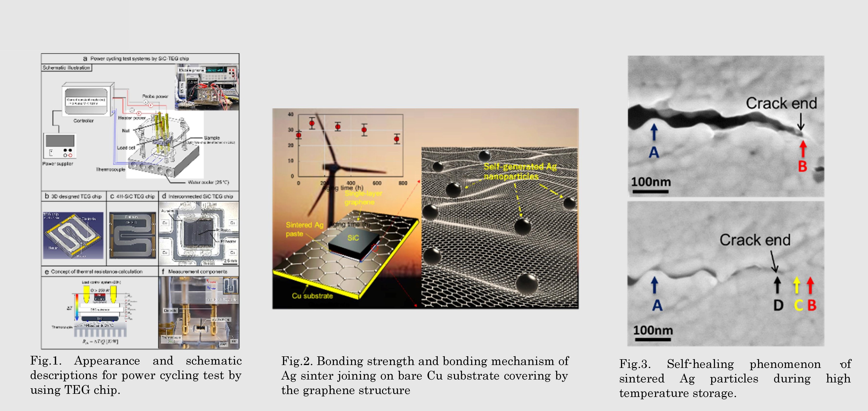
Fig.2. Bonding strength and bonding mechanism of Ag sinter joining on bare Cu substrate covering by the graphene structure
Fig.3. Self-healing phenomenon ·of sintered Ag particles during high temperature storage.
文献 / Publications
C. Chen,et.al, Scripta. Mater.,179 (2020) 36-39; C. Chen, et.al, Mater. Design., 162 (2019) 311-321; C. Chen, et.al, Appl Surf Sci., 497 (2019) 143797;C. Chen,et.al, Scripta. Mater., 146 (2018) 123-127; C. Chen, et.al, Acta Mater., 129 (2017) 41-51; C. Chen, et.al, Appl Phys Lett., 109 (2016) 093503.
研究者HP
- chenchuantong
 sanken.osaka-u.ac.jp
 - https://www.eco.sanken.osaka-u.ac.jp/
- http://www.f3d.sanken.osaka-u.ac.jp/