RIES
Research Institute for Electronic Science, Hokkaido University
北海道大学
電子科学研究所
LAST UPDATE 2017/02/25
-
研究者氏名
Researcher Name近藤憲治 Kenji KONDO
准教授 Associate Professor -
所属
Professional Affiliation北海道大学電子科学研究所
物質科学研究部門 ナノ構造物性研究分野
Research Institute for Electronic Science, Hokkaido University
Material and Molecular Sciences, Laboratory of Nanostructure Physics -
研究キーワード
Research Keywords物性理論
スピントロニクス
半導体デバイス工学
自己無撞着電子構造計算
Condensed Matter Theory
Spintronics
Semiconductor device engineering
First principle electronic structure calculation
- 研究テーマ
Research Subject -
新規なスピントロニクス・デバイスの探索および低次元電子ガスのエネルギースペクトラムの研究
Search for novel spintronics devices and study of exact energy spectrum of low dimensional electron gas
研究の背景 Background
リソグラフィーを利用した微細構造作製技術の限界によりCMOS素子によるLSI回路は集積化の限界に直面している。その結果、CMOS素子とは異なる動作によってCMOS素子を超えるデバイスを作製しようという試みが世界中で行われており、beyondCMOSと呼ばれている。スピントロニクスは、そのような要請の中で現れた新しい研究分野である。また集積化において、電子は低次元の系に閉じ込められることが多くなり、新規なデバイスの開発や新しい物理の発見にとって、電子相関の強い系での電子構造を正確に知ることが重要になっている。
The LSI circuit faces CMOS scaling limits that comes from the limits of micro-fabrication using optical lithography. As a result, the research has been conducting for seeking the candidate devices which overcome the limits all over the world. The devices are called beyond CMOS devices. Spintronics is a new research field that could replace the electronics. Also, electrons are frequently confined within very small region due to the integration, resulting in the strong correlation among electrons. It is very important to investigate the exact energy spectrum of such electron systems for developing novel devices and/or discovering new physical phenomena.
研究の目標 Outcome
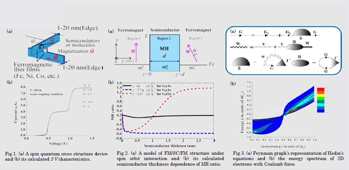
新規なスピントロニクス・デバイスを考案し、そのスピン伝導特性を明らかにし、それを実験家の方と実現していく。スピン軌道相互作用はSU(2)の非可換ゲージ場と見なせ、そのために位相不変量が付随することが多いので、その位相不変量を利用したデバイスの提案・開発を行いたい。一方、集積化に伴い低次元化を余儀なくされる電子の1電子スペクトラムをGW近似やGWΓ近似を用いて、正確に計算する。その際にスピン軌道相互作用の影響を取り込んだ計算を行う。これは、最終的には密度汎関数法の交換・相関カーネルにまで昇華させたい。
I try to seek for novel spintronics devices and clarify their characteristics of spin transport theoretically, and realize the device with experimentalist. Spin orbit interaction can be regarded as non-abelian SU(2) gauge field. As a result, topological invariants are frequently associated with it. I would like to invent a novel device which utilizes the topological invariants. On the other hand, I try to calculate oneparticle energy spectrum of low-dimensional electron systems using GW and GWΓ approximations, taking into consideration spin orbit interaction. I hope that this calculation will lead to exchange-correlation kernel of density functional theory
研究図Research Figure
文献 / Publications
J. Appl. Phys., 115, 17C701 (2014). J. Appl. Phys., 115, 17B901 (2014). Jpn. J. Appl. Phys., 52, 013001 (2013). Appl. Phys. Lett., 101, 32411 (2012). J. Appl. Phys., 111, 07C713 (2012). 解説:「ホール効果と異常ホール効果, そしてその先にあるもの」, 日本金属学会誌 まてりあ 48, 55 (2009). Jpn. J. Appl. Phys., 45, 9137 (2006).
研究者HP
- kkondo
 es.hokudai.ac.jp
 - http://qed4.es.hokudai.ac.jp/kondo.htm
- http://qed4.es.hokudai.ac.jp/en/kondo.htm