
SANKEN
The University of Osaka
大阪大学
産業科学研究所
LAST UPDATE 2020/06/18
-
研究者氏名
Researcher Name菅沼克昭 Katsuaki SUGANUMA
特任教授 Specially Appointed Professor -
所属
Affiliation大阪大学 産業科学研究所
フレキシブル3D実装協働研究所(所長)
SANKEN, The University of Osaka
F3D Collaborative Research Institute(Director) -
研究キーワード
Research Keywordsプリンテッドエレクトロニクス材料
異種材料接合技術
パワーエレクトロニクス実装材料
Printed electronics materials
Interconnection materials
Power electronics interconnection
Beyond 5G
- 研究テーマ
Research Subject -
先端エレクトロニクス機器の新実装材料とプロセス開発
Interconnection materials and process development for advanced electronics
研究の背景 Background of the Research
ウェアラブル・デバイスは、人ばかりでなくあらゆる「物」にまで違和感なく装着されることで、今後の高齢化社会に対応するヘルスケア、自動車、スマートハウスなどの、快適な生活空間開拓のための主役になる。このためには、可撓性ばかりでなく伸張性も必須な特性となり、従来のデバイス実装技術では及ばない、低温プロセス、低コスト、ストレッチャブル性付与などの技術開発が必要である。一方、人類の大きな課題であるエネルギー問題の解決には、全てのエネルギー変換における膨大なロスをSiCやGaNなどのワイドバンドギャップ(WBG)・パワー半導体の実現が望まれている。
Wearable devices have been expanding its market into wide area such as healthcare, automobile, and smart houses in recent years. For further development, stretchability is required in addition to flexibility and, therefore, a technology for low temperature process, stretchable interconnection as well as affordability should be established. On the other hand, energy crisis is another technological issue to be solved at the first priority. WBG semiconductors are expected to be one of the key solutions for this.
研究の目標 Research Objective
当研究室では、新たな世界を切り開くウェアラブル・デバイスと省エネルギー技術の切り札であるWBGパワー半導体を社会実装するために、ナノ材料・プロセス開発と同時に、ミクロ、マクロまでの組織制御に取り組み、さらに、デバイスの高信頼化のために、デバイス劣化メカニズムを理解するためのナノレベルの現象解明、評価技術の開発を進めている。また、産業界で必要な評価基準を定め、高信頼性デバイス市場を確固とするためのISOやIEC等の国際標準化を行っている。
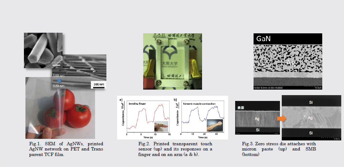
Wearable and transparent devices by using metallic nanowires, which are ultra-flexible and -stretchable, have been developed in order to realize the IoT world. A new idea for assembling WBGs has been demonstrated as “Zero stress die attach”. The reliability analysis has been carried out from nanoscale to macroscopic. International standardizations have been strongly promoted to support these new technology.
研究図Figures
論文発表 / Publications
・ Ultra thermal stability of LED die-attach achieved by pressureless Ag stress-migration bonding at low temperature, Acta Matel., (2015), in press.
・ Miniaturized flexible antenna printed on high dielectric constant nanopaper composite, Adv. Mater., (2015), in press.
研究者連絡先 / HP
- suganuma
 sanken.osaka-u.ac.jp
 - http://www.eco.sanken.osaka-u.ac.jp/
- http://www.f3d.sanken.osaka-u.ac.jp/#/