
IMRAM
Institute of Multidisciplinary Research for Advanced Materials, Tohoku University
東北大学
多元物質科学研究所

LAST UPDATE 2021/05/05
-
研究者氏名
Researcher Name秩父重英 Shigefusa CHICHIBU
教授 Professor -
所属
Affiliation東北大学 多元物質科学研究所
計測研究部門・量子光エレクトロニクス研究分野
Institute of Multidisciplinary Research for Advanced Materials, Tohoku University
Division of Measurements, Quantum Optoelectronics Laboratory -
研究キーワード
Research Keywords光半導体物性・デバイス
量子ナノ構造形成
時間・空間分解 発光スペクトロスコピー
Optical properties of condensed matter, Optical devices
Quantum nanostructures
Temporally / Spatially resolved emission / carrier dynamics
- 研究テーマ
Research Subject -
ワイドバンドギャップ半導体量子構造創成と時間・空間分解スペクトロスコピー
Development of ultra wide bandgap semiconductor materials and devices
研究の背景 Background of the Research
光子系(電磁波)と電子系(励起子)の機能を融合する新奇デバイス等を提案し、半導体デバイスの省エネルギー性能を飛躍的に向上させ、CO2排出量削減によりSDGsに貢献する。特に、禁制帯幅波長が200nm台の深紫外線発光機器を小型固体デバイス化することにより、殺菌や水の浄化、固体励起等の分野で人間生活に貢献できる。このため、バンドギャップの広い半導体のナノ超薄膜を基本とするデバイス構造のエピタキシャル形成を行い、それらの発光性能を正しく評価する必要がある。
Research objectives are to design and create quantum nanostructures desirable for environment-friendly functional optoelectronic devices, especially workable in deep ultraviolet wavelengths, based on wide bandgap semiconductors. Ultrafast recombination dynamics of excited particles in these structures are studied by time-resolved spectroscopy, and local luminescence properties are proved by spatially-resolved luminescence techniques. We eventually contribute to SDGs for our lives.
研究の目標 Research Objective
BN,AlN,GaN,InN等のⅢ族窒化物半導体やNiO,MgZnOなどの酸化物半導体の超薄膜積層構造を有機金属気相エピタキシー法、ヘリコン波励起プラズマスパッタエピタキシー法等によって形成し、フェムト秒レーザによる超短パルス光励起やフェムト秒レーザ励起集束電子線励起による時間・空間同時分解分光法などを通じて微細領域における励起子の物性(発光ダイナミクス等)を明らかにし、新たな光・電子デバイスを提案します。
We are growing quantum structures based on wide bandgap (B, Al, In, Ga)N, NiO, and (Mg, Zn)O semiconductors by metalorganic vapor phase epitaxy (MOVPE) and unique helicon-wave-excited-plasma sputtering epitaxy (HWPSE) methods. Ultrafast recombination dynamics are studied by deep ultraviolet temporally resolved photoluminescence, spatially resolved cathodoluminescence, and spatio-time-resolved cathodoluminescence system equipped with a home-made focused pulsed electron gun.
研究図Figures
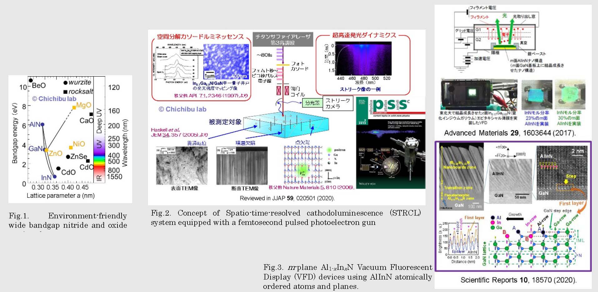
Fig.2. Concept of Spatio-time-resolved cathodoluminescence (STRCL) system equipped with a femtosecond pulsed photoelectron gun
Fig.3. m-plane Al1-xInxN Vacuum Fluorescent Display (VFD) devices using AlInN atomically ordered atoms and planes.
論文発表 / Publications
J. Appl. Phys. 135, 185701 (2024). Sci. Rep. 14, 169 (2024). Appl. Phys. Lett. 122, 201105 (2023). Appl. Phys. Lett. 119, 182106 (2021). Jpn. J. Appl. Phys. 61, 050501 (2022). Sci. Rep. 10, 18570 (2020). Appl. Phys. Lett. 117, 071103 (2020). J. Appl. Phys. 127, 215704 (2020). Appl. Phys. Lett. 113, 191901 (2018).
研究者連絡先 / HP
- chichibu
 tohoku.ac.jp
 - https://www2.tagen.tohoku.ac.jp/lab/chichibu/html/index-j.html