SANKEN
The University of Osaka
大阪大学
産業科学研究所
LAST UPDATE 2025/04/15
-
研究者氏名
Researcher Name楊金峰 Jinfeng YANG
准教授 Associate Professor -
所属
Affiliation大阪大学 産業科学研究所
先進ナノファブリケーション研究分野
SANKEN, The University of Osaka
Department of Advanced Nanofabrication -
研究キーワード
Research Keywordsアト秒・フェムト秒電子線パルス
パルスラジオリシス
超高速電子線回折・電子顕微鏡
超高速現象の解明
Attosecond/femtosecond electron pulses
Pulse radiolysis
Ultrafast electron diffraction/microscopy
Ultrafast phenomena and dynamics
- 研究テーマ
Research Subject -
相対論的フェムト電子線パルスを用いたフェムト秒原子イメージングの研究
Femtosecond atomic imaging with relativistic femtosecond electron pulses
研究の背景 Background of the Research
近年、物質の構造相転移、電荷・エネルギー移動、化学反応等のナノ領域に特有な高速物理・化学現象に基づいた新たな物質の設計とその応用が大きな注目を集めています。物質における高速現象を解明するためには、物理・化学的な素過程を支配する原子や分子の運動の観察が不可欠であり、時間的にフェムト秒(10の-15乗秒)、空間的にナノメートル以下の領域での測定技術が要求されている。
Recently, ultrafast phenomena in materials such as phase transitions, charge/energy transformations and chemical reactions are a significant and growing interest in designing new materials and devices for application. To understand such ultrafast phenomena, the motion of atoms or molecules in the physics-chemical processes in matter is necessary to be observed directly. A measurement technique with femtosecond temporal resolution and sub-nanometer spatial resolution has long been a goal for the scientists.
研究の目標 Research Objective
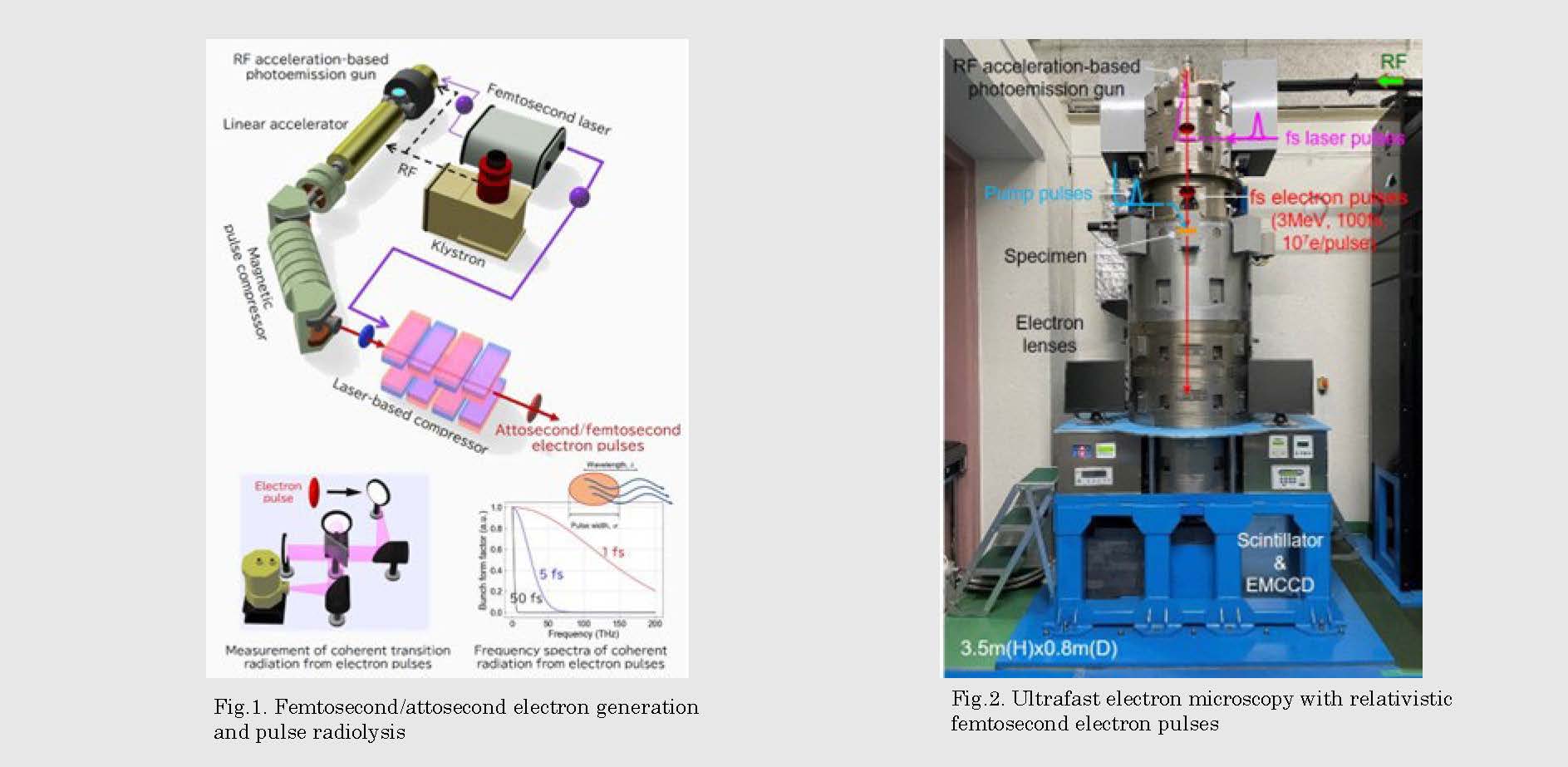
本研究では、フェムト秒レーザーと高周波(RF)加速器の技術を融合して相対論的フェムト秒・アト秒電子線パルスを発生し、フェムト秒時間分解能を有する光吸収分光測定法(パルスラジオリシス)と超高速電子顕微鏡法の開発を行っている。これらのフェムト秒時間分解計測技術を用いて、物質中の電子や原子の動きを探ることで、化学反応と構造変化が起きる瞬間、中間活性種や新しい物質構造の生成過程、機能発現メカニズム等を調べ、次世代半導体材料や微細加工プロセスの開発、新機能性材料・デバイスの創製への貢献を目指しています。
We are developing two femtosecond time-resolved measurement techniques with relativistic attosecond/femtosecond electron pulses. One is pulse radiolysis for the study of ultrafast physicochemical reactions in materials. Another is ultrafast electron microscopy to observe structural dynamics directly in nanomaterials and nanodevices. The studies are encouraged to gain a deeper understanding of nanomaterials and to achieve a novel breakthrough in materials science.
研究図Figures
論文発表 / Publications
Optics Express, 32, 23180 (2024). STAM, 24, 2150525 (2022). Quantum Beam Science, 4, 4 (2020). Advances in Condensed Matter Physics, 2019, 9739241(2019). Microscopy, 67, 291(2018). Appl. Phys. Lett. 103, 253107(2013); 98, 251903(2011). Phys. Rev. B 88, 184101(2013).
研究者連絡先 / HP
- yang
 sanken.osaka-u.ac.jp
 - http://www.sanken.osaka-u.ac.jp/labs/bsn/index.html