
IMCE
Institute for Materials Chemistry and Engineering, Kyushu University
九州大学
先導物質化学研究所

LAST UPDATE 2023/08/08
-
研究者氏名
Researcher Name梶野祐人 Yuto KAJINO
助教 Assistant Professor -
所属
Affiliation九州大学 先導物質化学研究所
物質基盤化学部門・ナノ界面物性分野
Institute for Materials Chemistry and Engineering, Kyushu University
Division of Fundamental Organic Chemistry/ Nanomaterials and Interfaces -
研究キーワード
Research Keywords低次元物質の光物性
プラズモニクス
ナノフォトニクス
Optical properties of low–dimensional materials
Plasmonics
Nanophotonics
- 研究テーマ
Research Subject -
低次元半導体ハイブリッドナノ構造における新奇光物理の開拓
Optical physics in hybrid nanostructures of low-dimensional semiconductors
研究の背景 Background of the Research
半導体ナノ材料は、量子閉じ込め効果などその低次元構造に由来した特異な光―物質相互作用を示し、これまで広く研究が行われてきた。また、大きな比表面積を持つことから、周囲環境がその物質自身の性質に大きな影響を与える。そのため、周囲材料やナノ材料自身の配列構造を適切に制御することで、多様な物性制御が可能である。加えて、このような物性制御手法は、ナノデバイス開発に対する重要な知見を提供するのみならず、異種ナノ材料とのハイブリッド構造形成により従来ない革新的な光物理の発現が期待される。
Semiconductor nanomaterials exhibit unique optical properties, such as the quantum confinement effect. Moreover, owing to their large surface area-to-volume ratio, the surrounding environment significantly influences their inherent properties. Thus, by controlling the arrangement of nanomaterials and their surrounding materials, diverse property manipulations can be achieved. These tunabilities offer not only valuable insights into the development of optimal nanodevices, but also hold promise for the emergence of innovative optical phenomena through the formation of hybrid structures with heterogeneous nanomaterials.
研究の目標 Research Objective
半導体の性質を有するナノ粒子(量子ドット)・単原子層材料と、金属・絶縁体ナノ材料とのハイブリッドナノ構造の形成及び自在な構造・物性制御手法を確立する。また、半導体ナノ粒子のホモ集積構造、ヘテロ複合体形成に伴う光学特性変化について、複数の分光手法(顕微分光、レーザー分光)とナノ構造観察手法(AFM、SEM、TEM)とを組み合わせたその物理機構解明を目指す。最終的には、半導体を主要な構成要素としたハイブリッドナノ複合体における光物理の学理を構築する。
We establish to fabricate and control hybrid nanostructures that incorporate semiconductor nanocrystals and monolayers with metals and insulators. In addition, we elucidate the physical mechanisms behind the changes in optical properties that accompany the formation of homogeneously assembled structures and hetero complexes. This will be achieved through the combination of various spectroscopic methods (micro spectroscopy, laser spectroscopy) and nanostructure observation techniques (AFM, SEM, TEM). Ultimately, our goal is to construct a principle for optical physics in hybrid nanocomposites , primarily composed of semiconductor nanomaterials.
研究図Figures
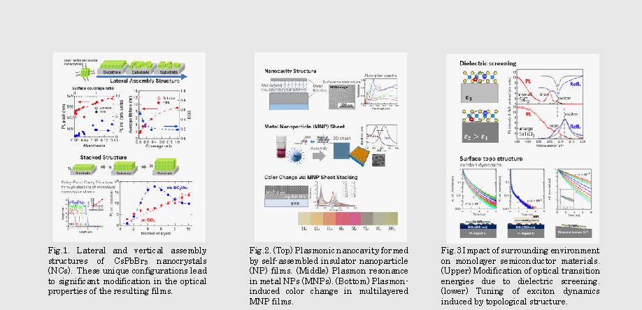
Fig.2. (Top) Plasmonic nanocavity formed by self-assembled insulator nanoparticle (NP) films. (Middle) Plasmon resonance in metal NPs (MNPs). (Bottom) Plasmon-induced color change in multilayered MNP films.
Fig.3 Impact of surrounding environment on monolayer semiconductor materials. (Upper) Modification of optical transition energies due to dielectric screening. (lower) Tuning of exciton dynamics induced by topological structure.
論文発表 / Publications
Phys. Rev. Materials 6, L043001 (2022). Journal Phys. Rev. B, 103, L241410 (2021). J. Phys. Chem. C 123, 14097 (2019). Adv. Optical Mater. 11, 2202326 (2023). Nanoscale, 14, 9278 (2022).
研究者連絡先 / HP
- kajino
 ms.ifoc.kyushu-u.ac.jp
 - https://www.cm.kyushu-u.ac.jp/ktamada/