RIES
Research Institute for Electronic Science, Hokkaido University
北海道大学
電子科学研究所
LAST UPDATE 2023/01/20
-
研究者氏名
Researcher Name曲勇作 Yusaku MAGARI
助教 Assistant Professor -
所属
Professional Affiliation北海道大学電子科学研究所
附属グリーンナノテクノロジー研究センター
Research Institute for Electronic Science, Hokkaido University
Green Nanotechnology Research Center -
研究キーワード
Research Keywords高移動度酸化物半導体
薄膜トランジスタ
フレキシブルデバイス
High-mobility oxide semiconductors
Thin film transistors
Flexible devices
- 研究テーマ
Research Subject -
高移動度酸化物薄膜トランジスタ
High-mobility oxide thin-film transistors
研究の背景 Background
代表的な酸化物半導体である非晶質InGaZnO(IGZO)は、非晶質シリコンに比較して、高い電界効果移動度(~10 cm2 V−1 s−1)、極めて低いリーク電流、優れた大面積均一性等により、次世代ディスプレイや集積回路用途で活発な研究がなされ、実用化が始まりつつある。しかしながら、多結晶シリコン(~100 cm2V-1s-1)との比較や酸化物半導体の用途拡大のためには更なる高性能(高移動度)化が強く求められている。
Amorphous oxide semiconductors have been extensively studied as active channel layers of thin-film transistors (TFTs) for backplane of LCDs and OLED displays. This is because AOSs represented by amorphous In–Ga–Zn–O (a-IGZO) has properties that are superior to hydrogenated amorphous Si (a-Si:H), such as a large field-effect mobility (μFE) of over 10 cm2 V−1 s−1, an extremely low leakage current. Although the μFE value of a-IGZO TFTs is more than ten times higher than that of a-Si:H TFTs (<1 cm2 V−1 s−1), the further improvement of μFE values is required to expand their range of applications as alternatives to poly-Si TFTs (~100 cm2 V−1 s−1).
研究の目標 Outcome
我々は、多結晶シリコンを凌ぐ高移動度酸化物薄膜トランジスタの実現に向けて研究を行っている。近年、水素濃度を制御した多結晶In2O3:H 膜において、格子像が確認できる優れた結晶性を低温(~300℃)で実現しつつ、金属的伝導から半導体伝導にキャリア濃度を制御する手法を見いだし、世界最高性能酸化物薄膜トランジスタ(139.2 cm2 V−1 s−1)を実現した。In2O3:H TFTの高移動度の起源を解明し、次世代ディスプレイや半導体メモリーの高性能・低電力化、さらには透明フレキシブルデバイスの実現を目指している。
Our challenge is to boost a mobility (>100 cm2 V−1 s−1) of oxide TFTs as an alternative to poly-Si TFTs. Recently, we reported a μFE value of 139.2 cm2 V−1 s−1 for a TFT obtained using hydrogenated polycrystalline In2O3 (In2O3:H) formed via solid-phase crystallization at 300 °C. We believe that these In2O3:H TFTs are promising candidates for use in future display, memory, and sensor applications.
研究図Research Figure
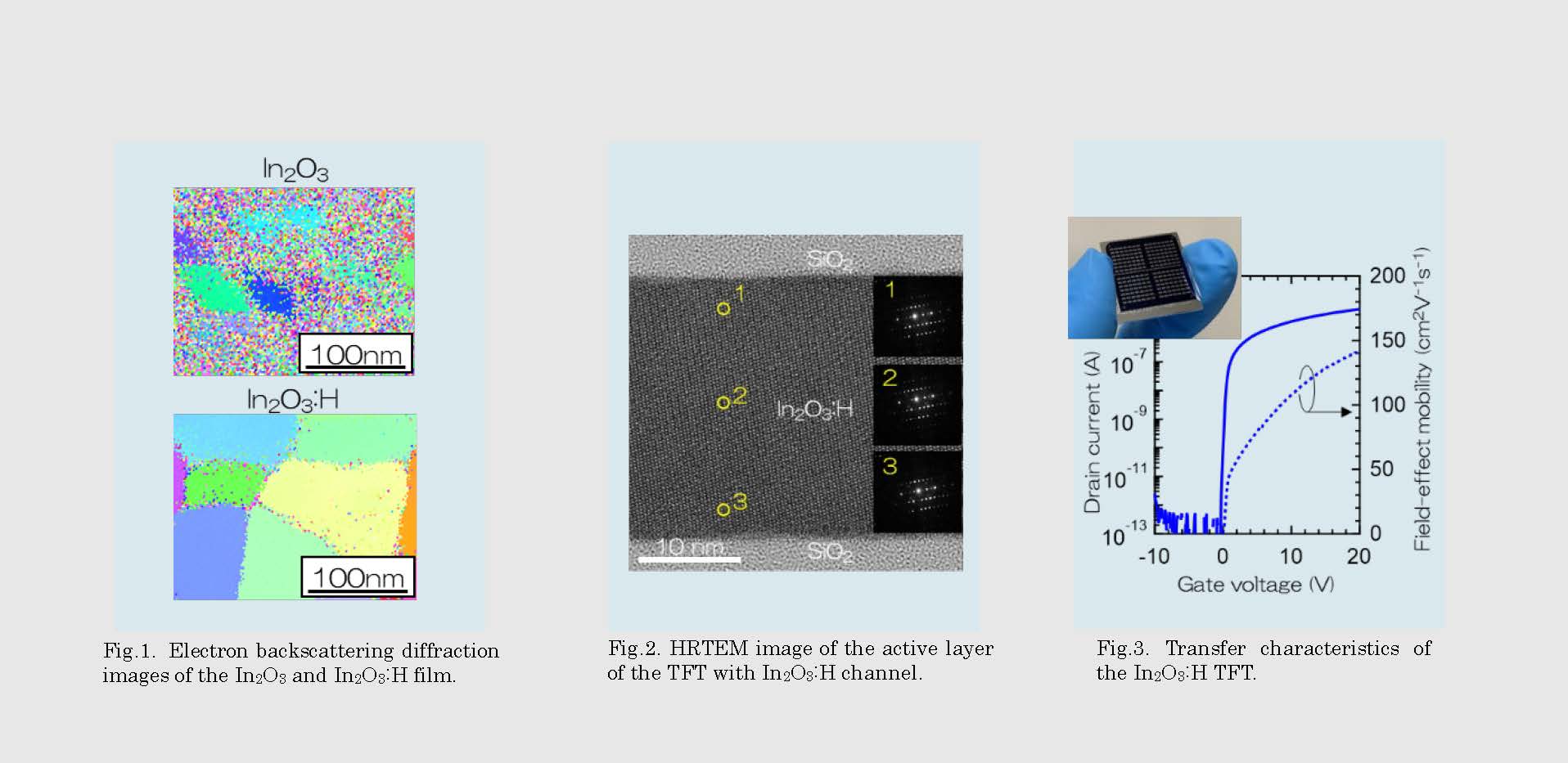
Fig.2. HRTEM image of the active layer of the TFT with In2O3:H channel.
Fig.3. Transfer characteristics of the In2O3:H TFT.
文献 / Publications
Nature Commun. 13, 1078 (2022)
研究者HP
- magari.yusaku
 es.hokudai.ac.jp
 - https://functfilm.es.hokudai.ac.jp/