RIES
Research Institute for Electronic Science, Hokkaido University
北海道大学
電子科学研究所
LAST UPDATE 2023/01/05
-
研究者氏名
Researcher Name岡本拓也 Takuya OKAMOTO
助教 Assistant Professor -
所属
Professional Affiliation北海道大学電子科学研究所
フォトニックナノ材料研究分野
Research Institute for Electronic Science, Hokkaido University
Laboratory of Photonic Nanomaterials -
研究キーワード
Research Keywords光物理化学
ハロゲン化鉛ペロブスカイト
ナノ粒子
励起子
Photo-physic chemistry
Lead halide perovskite
Nanoparticles
Exciton
- 研究テーマ
Research Subject -
ハロゲン化鉛ペロブスカイト結晶における構造と励起子挙動の制御
Structure- and excitonic property-control in lead halide perovskite crystals
研究の背景 Background
ハロゲン化鉛ペロブスカイトはハロゲン組成により蛍光波長を調整でき、高い蛍光量子収率を示すことから次世代発光材料として期待されている。これまで我々はナノ結晶や薄膜、マイクロ結晶など様々なペロブスカイト材料の光学機能について研究を進めてきた。現在はペロブスカイトナノ材料の集合および外部刺激による励起子挙動変化に関する研究に取り組んでいる。
Lead halide perovskites are promising and cost-effective semiconductor materials for next-generation optoelectronic applications due to their halide-dependent tunable band gap and high fluorescence quantum yields. We have investigated the optical properties of various perovskite materials such as nanocrystals, thin films, and microcrystals. We are studying the change of excitonic properties of perovskite nanomaterials by assembly formation and external stimuli.
研究の目標 Outcome
ペロブスカイトナノ結晶の超構造体(超結晶)を形成し、粒子集合や外部刺激などによる集積構造の変化をもとにペロブスカイト超結晶の励起子挙動の制御法を確立する。超結晶を構成するナノ結晶のサイズや粒子間距離、粒子配列などの「構造」と、超結晶における蛍光の波長や寿命、強度などの蛍光特性を支配する「励起子挙動」の関係を明らかにする。
We aim to establish the methods of controlling the excitons and carrier recombination in perovskite supercrystals based on their structural changes caused by assembly formation and external stimuli. We also aim to elucidate the relationship between the "structure" of perovskite supercrystals (size, interparticle distance, and particle arrangement), and the "excitonic properties" being related to the photoluminescence (PL) properties (PL wavelength, lifetime, and intensity).
研究図Research Figure
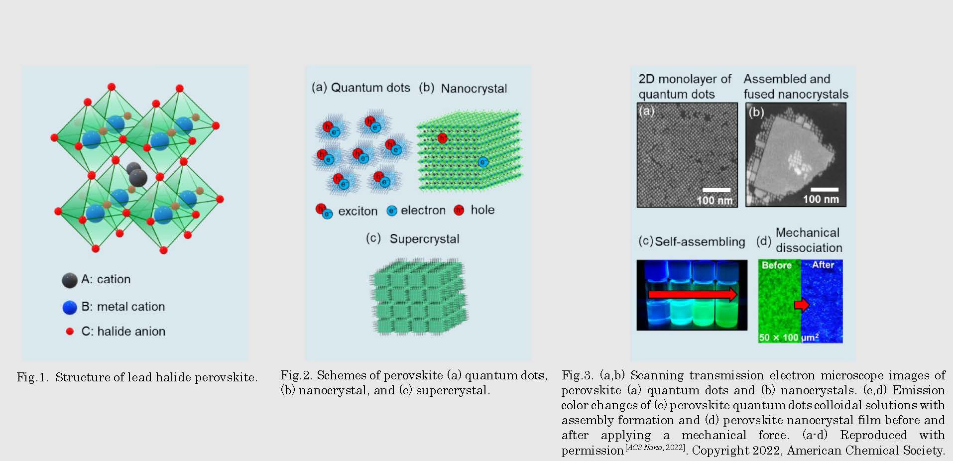
Fig.2. Schemes of perovskite (a) quantum dots, (b) nanocrystal, and (c) supercrystal.
Fig.3. (a,b) Scanning transmission electron microscope images of perovskite (a) quantum dots and (b) nanocrystals. (c,d) Emission color changes of (c) perovskite quantum dots colloidal solutions with assembly formation and (d) perovskite nanocrystal film before and after applying a mechanical force. (a-d) Reproduced with permission[ACS Nano, 2022]. Copyright 2022, American Chemical Society.
文献 / Publications
Adv. Mater. Technol., 2021, 6, 2000934.; Adv. Opt. Mater., 2021, 9, 2100355.; J. Phys. Chem. Lett., 2021, 12, 8644–8651.; ACS Nano, 2022, 16, 160–168; Angew. Chem. Int. Ed. 2022, 62, 4, e202215947.; Nanoscale 15(17) 7695-7702.; Small, 2023, 2303496.
研究者HP
- okamotot
 es.hokudai.ac.jp
 - http://bijulab.main.jp/en/