SANKEN
The University of Osaka
大阪大学
産業科学研究所
LAST UPDATE 2017/02/26
-
研究者氏名
Researcher Name大岩顕 Akira OIWA
教授 Professor -
所属
Affiliation大阪大学 産業科学研究所
第1研究部門・量子システム創成研究分野
SANKEN, The University of Osaka
Division of Information and Quantum Sciences, Quantum System Electronics -
研究キーワード
Research Keywords半導体低次元量子物性
光-スピン量子インターフェース
半導体スピントロニクス
Semiconductor low-dimensional quantum physics
Photon-spin quantum interface
Semiconductor spintronics
- 研究テーマ
Research Subject -
スピンと光を用いた革新的な量子複合素子の研究
Innovative hybrid quantum devices based on spins and photons
研究の背景 Background of the Research
近年、半導体や金属の微細加工技術の進展により、多彩な量子効果が実験室で研究できるようになっています。こうした量子効果は、低消費電力デバイスや新しい概念で動作する次世代デバイスにつながる可能性を秘めています。特に電子の持つスピンという性質は固体の普遍的な性質であり、その自由度を利用したスピントロニクスや量子計算は基礎と応用の両方で活発な研究分野である。
Recently, the development in the micro-fabrication technologies for semiconductors and metal enables one to realize the variety of phenomena based on quantum mechanics. Such quantum effect would potentially bring the low-power consumption devices and future devices operating with novel concept. In particular, electron spin is a universal nature in solid and the spintronics and quantum computation, which use the spin degree of freedom, has become research areas attractive for both basic science and applications.
研究の目標 Research Objective
半導体を中心に,電子スピンや光子の量子力学的性質を利用した量子情報処理や、新しい光・電子・スピン材料の創製と融合に基づいたスピントロニクスが研究の主な舞台です。高品質材料の創製から評価、そして精密な量子輸送測定まで一貫して行い、光、電子、スピンの自由度を自由に操る量子ナノ構造がもたらす新しい現象の発見を目指しています。
Based on semiconductor devices, our research fields are quantum information processing using the quantum mechanical nature of electron spins and photons, and spintronics based on the development and hybridization of optical, electrical and spin materials. We study the growth and characterization of high quality materials and perform precise quantum transport measurements. Aim of our research is the realization of novel phenomena emerging in quantum nanostructures that can control the photon, electron and spin degrees of freedom.
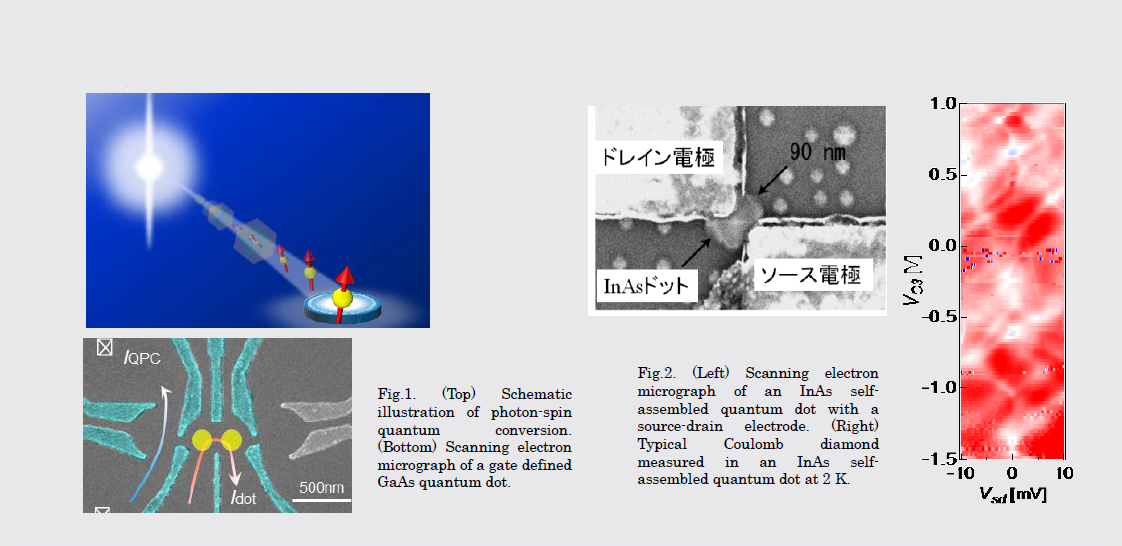
研究図Figures
論文発表 / Publications
Nature Nanotechnology 6, 511 (2011). Phys. Rev. Lett. 110, 226803 (2013). Applied Physics Letters 104, 263101 (2014). Nature communications 6, 7446 (2015).
研究者連絡先 / HP
- oiwa
 sanken.osaka-u.ac.jp
 - http://www.sanken.osaka-u.ac.jp/labs/qse/