ISIR
The Institute of Scientific and Industrial Research, Osaka University
大阪大学
産業科学研究所
LAST UPDATE 2017/02/26
-
研究者氏名
Researcher Name今村健太郎 Kentaro IMAMURA
助教 Assistant Professor -
所属
Professional Affiliation大阪大学産業科学研究所
半導体材料・プロセス研究分野
The Institute of Scientific and Industrial Research, Osaka University
Department of Semiconductor Materials and Processes -
研究キーワード
Research Keywords結晶シリコン太陽電池
シリコンナノクリスタル
シリコン微細加工
光学解析
Crystalline Si solar cells
Si nanocrystals
Micro-fabrication of Si
Optical analysis
- 研究テーマ
Research Subject -
シリコン表面のナノ構造化による極低反射化とシリコン太陽電池への応用
Fabrication of nano-structured Si surfaces with ultra-low reflectivity and its application to Si solar cells
研究の背景 Background
大部分の半導体製品に用いられるシリコンは現代社会に不可欠な材料です。特に結晶シリコン太陽電池は、市販される太陽電池の85%以上を占める重要な太陽電池であり、高効率な結晶シリコン太陽電池を低コストプロセスで作製することは地球環境問題への解決にとって非常に重要です。
Silicon is widely used in semiconductor products, and thus it is indispensable for modern society. Especially, crystalline Si solar cells have more than 85 % of the market share of commercial solar cells, and therefore, it is very important for solving global environmental problems to produce high conversion efficiency Si solar cells with low cost process.
研究の目標 Outcome
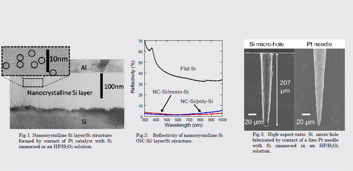
シリコンは、ナノサイズ化されると、本来のバルクとは異なる魅力的な特性を示します。例えばシリコン表面にシリコンナノクリスタル層を形成すると、表面反射率を40%から3%以下に低減可能です。我々は新規化学的手法によりシリコンをナノ構造化し、その物性を解明することや、シリコン太陽電池や水素発生材料への応用を目指し研究を行っています。
Nanosized Si has various attractive characteristics which are different from those of bulk Si. One of the useful characteristics is ultra-low reflectivity which can be achieved by forming nanocrystalline Si layer on Si surfaces, i.e., the reflectivity of the Si surfaces decreases from 40% to less than 3%. Nanocrystalline Si layer is formed by use of our new chemical method. We are aiming to elucidate their physical properties, and to apply them to Si solar cells and to hydrogen generation materials.
研究図Research Figure
文献 / Publications
Appl. Phys. Lett., 103 (2013) 013110-1-4, J. Electrochem. Soc., 160 (2013) H443-H445, J. Appl. Phys., 112 (2012) 124322
研究者HP
- k.imamura
 sanken.osaka-u.ac.jp
 - http://www.sanken.osaka-u.ac.jp/labs/fcm/index.html