IMRAM
Institute of Multidisciplinary Research for Advanced Materials, Tohoku University
東北大学
多元物質科学研究所
LAST UPDATE 2021/05/03
-
研究者氏名
Researcher Name上杉祐貴 Yuuki UESUGI
助教 Assistant Professor -
所属
Professional Affiliation東北大学多元物質科学研究所
プロセスシステム工学研究部門 光物質科学研究分野
Institute of Multidisciplinary Research for Advanced Materials, Tohoku University
Division of Process and System Engineering, Laser Applied Material Science -
研究キーワード
Research Keywordsポンデロモーティブレンズ
薄膜レーザー加工
光増強共振器
Ponderomotive lens
Laser processing of membrane
Optical enhancement cavity
- 研究テーマ
Research Subject -
先端レーザーを使った電子光学装置と薄膜レーザー微細加工技術の研究
Research on electron optical devices and laser-processing methods using advanced lasers
研究の背景 Background
先端のレーザー技術では、光の波長や強度、位相(波面)、偏光、時間構造などのパラメータを自由に制御することが可能です。近年、電子顕微鏡のレンズ素子を、電場や磁場のかわりに光で実現する技術が発案され、注目されています。また、すでに多くの応用展開が実現しているレーザー微細加工の分野でも、厚さがナノメートル程度の薄膜や、グラフェンに代表される二次元材料の加工は報告例が少なく、未開拓の領域でした。
Sophisticated laser technology offers many manipulation possibilities for light properties, such as wavelength, intensity, phase (wavefront), polarization, and temporal structure. Lately, a technology substituting electric or magnetic fields with light to create lens elements for electron microscopes has emerged, garnering significant interest. Even in the laser-processing field where numerous applications have been actualized, the machining of nanometer-thick membranes and two-dimensional materials such as graphene remains an unexplored field with limited studies.
研究の目標 Outcome
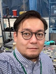
光と自由電子の2次の相互作用過程を利用する電子レンズとして、ポンデロモーティブレンズを世界に先駆けて提案しました[1,2]。このレンズは電子顕微鏡の球面収差補正に利用できる可能性があり、その実証に向けた研究に取り組んでいます。また、従来のナノ加工技術では取り扱いが困難だったナノ薄膜や単層グラフェンを、サブ100 nmの分解能で加工するレーザー加工技術を開発しました[3,4]。今後、最先端の半導体産業や量子科学・材料研究、生体センサー等への展開を目指していきます。
We proposed the world's first ponderomotive lens as an electron lens that utilizes the second-order interaction process between light and free electrons [1,2]. This lens has the potential for use in spherical aberration correction in electron microscopes. Furthermore, we have demonstrated the laser-processing that enables us to process nanomembranes and monolayer graphene with sub-100 nm resolution [3,4]. Our future aspirations involve broadening the application of this technique across various domains, including the advanced semiconductor industry, quantum and materials science, and advanced bio-sensors.
研究図Research Figure
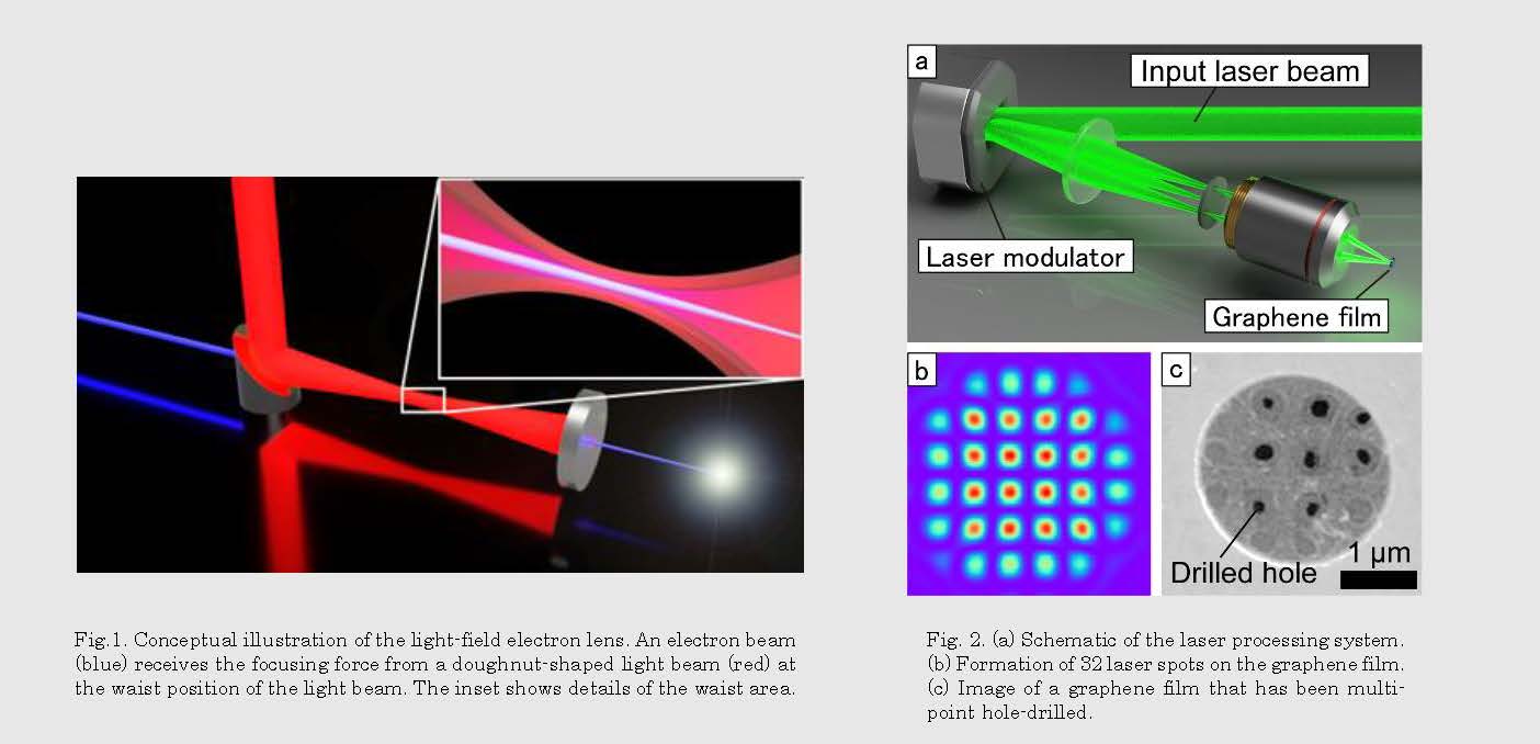
Fig. 2. (a) Schematic of the laser processing system. (b) Formation of 32 laser spots on the graphene film. (c) Image of a graphene film that has been multi-point hole-drilled.
文献 / Publications
[1] Y. Uesugi, Y. Kozawa, and S. Sato, Phys. Rev. Applied 16, L011002 (2021). [2] Y. Uesugi, Y. Kozawa, and S. Sato, J. Opt. 24, 054013 (2022). [3] Y. Uesugi et al., Appl. Phys. A 129, 101 (2023). [4] N. Kadoguchi et al., Nano Lett. (2023) (volume, issue, and pages to be determined).
研究者HP
- uesugi
 tohoku.ac.jp
 - http://satolab.tagen.tohoku.ac.jp