RIES
Research Institute for Electronic Science, Hokkaido University
北海道大学
電子科学研究所

LAST UPDATE 2018/10/26
-
研究者氏名
Researcher Name太田裕道 Hiromichi OHTA
教授 Professor -
所属
Professional Affiliation北海道大学電子科学研究所
附属グリーンナノテクノロジー研究センター
Research Institute for Electronic Science, Hokkaido University
Green Nanotechnology Research Center -
研究キーワード
Research Keywords酸化物熱電材料
透明酸化物半導体デバイス
熱電能電界変調法
全固体熱トランジスタ
Oxide thermoelectric materials
Transparent oxide semiconductor devices
Electric field thermopower modulation
Solid-state thermal transistors
- 研究テーマ
Research Subject -
セラミックス素材で役に立つモノを創ります
We develop useful devices using ceramics
研究の背景 Background
物質表面や異種物質の接合界面近傍における厚さ数ナノ㍍の領域は、仕事関数や化学ポテンシャルの差を解消し、熱平衡状態になるため、固体内部とは全く異なる電子状態になり、様々な興味深い電子・イオン伝導特性が生じると期待されます。しかし、機能性酸化物は、従来、セラミックスとして扱われ、その電気伝導性などにはあまり興味を持たれることがありませんでした。機能性酸化物の持つ真のポテンシャルを引出すためには、超精密な薄膜作製技術を駆使して作製される、原子レベルで平坦な表面を有する高品質薄膜が必要不可欠です。
Since the electronic structure at the surface and/or interface (several nanometers in thickness) of materials is completely different from the solid interior due to the differences of the work functions and chemical potential, surface and/or interface exhibits a variety of interesting electronic / ionic conductivity. However, electrical properties of functional oxides have not been utilized so far due to the lack of high-quality epitaxial films. High-quality epitaxial films with atomically flat surface, which can be fabricated by ultra-precise film growth technique, are necessary to extract their intrinsic potential.
研究の目標 Outcome
機能性酸化物の表面・界面で起こる興味深い現象を、単結晶薄膜を用いて解き明かし、モデル化することによる新しい材料設計指針の提案を目指しています。これまでに、酸化物人工超格子や電界効果トランジスタの二次元電子ガスなどの電子輸送特性、特に熱電効果について調査してきました。最近はイオン輸送にも興味を持ち、薄膜作製スキルを活かして異種接合界面を作製し、界面におけるイオン伝導の研究を開始したところです。将来役に立つ全固体薄膜デバイスの実現を目指します。
We propose novel material design concept of functional oxides by using high-quality epitaxial films, which enable us to clarify interesting phenomenon at the surface and/or interface. Electron transport properties, especially Seebeck effect, of two-dimensional electron gases in oxide superlattices and field effect transistors have been investigated so far. We are now focusing on ionic conductivity at heterointerfaces to realize all solid-state thin film devices near future.
研究図Research Figure
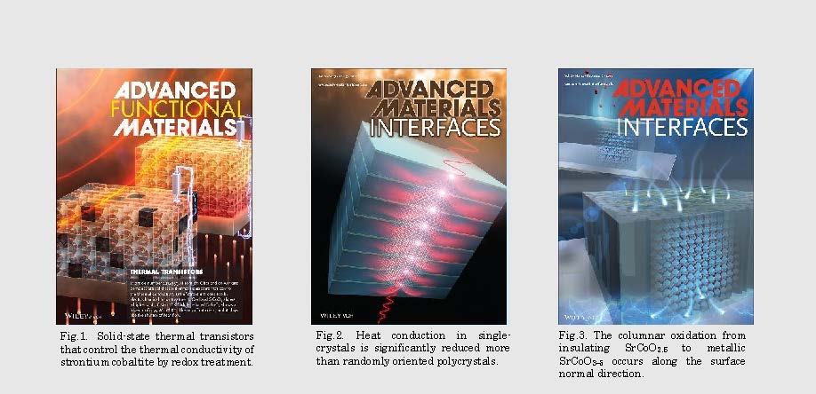
Fig.2. Heat conduction in single-crystals is significantly reduced more than randomly oriented polycrystals.
Fig.3. The columnar oxidation from insulating SrCoO2.5 to metallic SrCoO3−δ occurs along the surface normal direction.
文献 / Publications
Q. Yang, H. Ohta et al., Adv. Funct. Mater. 33, 202214939 (2023); H. Yang, H. Ohta et al., ACS Appl. Electron. Mater. 4, 5081 (2022); X. Zhang, H. Ohta et al., ACS Appl. Mater. Interfaces 14, 33355 (2022); X. Zhang, H. Ohta et al., ACS Appl. Mater. Interfaces 13, 54204 (2021); H.J. Cho, H. Ohta et al., Adv. Mater. Interfaces 2001932 (2021).
研究者HP
- hiromichi.ohta
 es.hokudai.ac.jp
 - https://functfilm.es.hokudai.ac.jp/