IMCE
Institute for Materials Chemistry and Engineering, Kyushu University
九州大学
先導物質化学研究所
LAST UPDATE 2017/02/25
-
研究者氏名
Researcher Name藤田克彦 Katsuhiko FUJITA
准教授 Associate Professor -
所属
Professional Affiliation九州大学先導物質化学研究所
先端素子材料部門・先端光機能材料分野
Institute for Materials Chemistry and Engineering, Kyushu University
Division of Advanced Device Materials, Photonic Materials -
研究キーワード
Research Keywords有機エレクトロニクス
高分子半導体
有機超薄膜
有機太陽電池
Organic electronics
Polymer semiconductor
Organic thin film
Organic photovoltaic cell
- 研究テーマ
Research Subject -
有機エレクトロニクスデバイス作製プロセスと材料の開発
Development of device fabrication process and materials in organic electronics
研究の背景 Background
従来の半導体デバイスはシリコン結晶をベースに微細加工技術の発展とともに発達してきました。対して柔らかい有機半導体を使った電子デバイスは素子自体を柔軟な構造にできるほか、印刷技術などの塗布プロセスで製造することで低コスト大面積での生産が可能になるとして注目を集めています。新しい材料やデバイス製造方法などの発達により性能が年々向上しており、次代の電子電気産業を担うものと期待されています。
Conventional semiconductor devices based on silicon crystal have been developed by the improvement of fine processing technology. On the other hand, soft organic semiconductor devices have significant advantage that they enable fabricating flexible devices and producing low-cost large area devices by use of printing technology. Nowadays, new materials and production technology have been developed and the device performance is getting improved rapidly. They are expecting to contribute the electronics industry in next generation.
研究の目標 Outcome
独自の有機半導体の成膜プロセスを開発し、従来は難しかった塗布プロセスでの半導体薄膜構造制御や、難溶性材料の素子化などを通じて、有機デバイスの高性能化や、連続プロセスでの超低コスト製造技術を開発することを目指しています。また、有機半導体特有の性質を利用した新しい電子デバイスを生み出すことにも注力しています。
The improvement of organic device performance and the development of low-cost fabrication process are aimed by invention of original thin layer deposition system using insoluble materials which cannot be used for the organic devices in conventional ways. The other objective of our research is development of new organic devices utilizing exclusive characteristics of organic semiconductors.
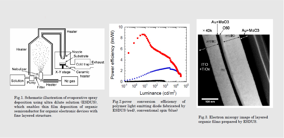
研究図Research Figure
文献 / Publications
Appl. Phys Let. 102, 023302 (2013). Jpn, J. Appl. Phys. 896,451(2014). Org. Electr. 10, 834 (2009). 機能材料, 28(6), 42-46 (2008).
研究者HP
- katsuf
 asem.kyushu-u.ac.jp
 - http://www.asem.kyushu-u.ac.jp/of/of03/jp/