ISIR
The Institute of Scientific and Industrial Research, Osaka University
大阪大学
産業科学研究所
LAST UPDATE 2017/02/26
-
研究者氏名
Researcher Name菅原徹 Tohru SUGAHARA
助教 Assistant Professor -
所属
Professional Affiliation大阪大学産業科学研究所
第二研究部門・先端実装材料研究分野
The Institute of Scientific and Industrial Research, Osaka University
Department of Advanced Interconnection Materials -
研究キーワード
Research Keywords熱電変換
太陽電池
金属有機化合物分解法
拡散制御と界面
Thermoelectric conversion
Photo voltaic
Metal organic decomposition method
Diffusion control and interface
- 研究テーマ
Research Subject -
金属有機化合物分解法を用いた印刷用インクの開発とエレクトロニクスデバイスの創出
Procreation of devices and development of metal organic decomposition inks for next generation printed electronics
研究の背景 Background
永続的持続可能な人類社会の実現において、低環境負荷に基づく工業廃棄物の削減や低材料資源化、低消費エネルギー化などが世界的に注目されている。印刷法を用いたデバイス作製技術は、プリンテッド・エレクトロニクス(PE)技術とよばれ、真空法やリソグラフィー法を使用しない体環境不可なデバイス作製プロセスとして材料とともに開発が盛んである。また、PE技術は、近未来のユビキタス社会実現に向けて、ウェアラブルを代表とする伸縮性や可塑性、透過性などの付加的価値を持った電子デバイス開発が積極的に取り組まれている。
To realize the permanent sustainable human society, industrial reducing waste products of raw materials, energy consumption and greenhouse gas emissions have gained global attention in the world. Printed electronics (PEs), which can be produced electronics devices by printing method is one of the emerging manufacturing technology expected to overcome these environmental issues. Moreover, PEs technology of materials and process is actively studying and developing intended to additional wearable functions, such as flexible, stretchable, and transparent properties.
研究の目標 Outcome
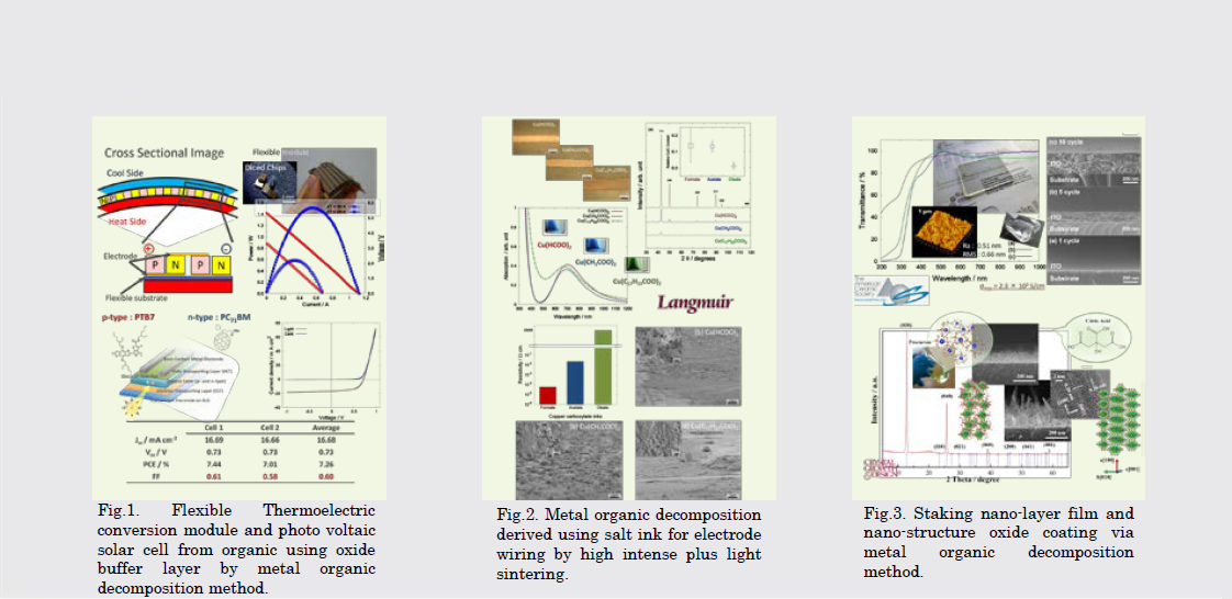
我々の研究グループでは、金属有機化合物分解法を中心に、PE技術用の半導体および配線用インクとその実装プロセスを開発している。これまで、有機金属塩を器質とした塩インクや酸化物半導体の前駆体インクを開発し、様々な方法で焼結している。今後の研究目標は、これらの技術を組み合わせることで、熱電変換モジュール、太陽電池、薄膜トランジスタなどのデバイスを作製するとともに、それらをアセンブリする回路設計と将来ユビキタス社会の実現に資するエレクトロニクスモジュールを開発する。
Very recently, the metal organic decomposition inks for semiconductor and electrode wiring as PEs technology have developed in our research group. The organic metal salt inks, especially, precursor of oxide semiconductor ink has been developed by a variety of sintering methods such as high intense pulsed photo-sintering. The goal of the future studies, the next generation electrics devices such as the thermoelectric conversion modules, the photo voltaic solar cells, and thin film transistors as well as with the functional properties are making by combining these techniques, which contribute to the realization of future ubiquitous human society.
研究図Research Figure
文献 / Publications
1) Cryst. Growth Des. (2015) in press (DOI: 10.1021/acs.cgd.5b00790).
2) J. Am. Ceram. Soc., 97, 10, 3238, 2014.
3) ACS Appl. Mater. Interfaces 6, 18, 16297, 2014.
4) Thin Solid Films, 565, 28, 11, 2014.
5) Langmuir, 29, 11192 2013.
6) J. Mater. Chem., 22, 23561, 2012.
7) Appl. Phys. Lett. 99, 062107, 2011.
研究者HP
- sugahara
 sanken.osaka-u.ac.jp
 - http://www.eco.sanken.osaka-u.ac.jp/