ISIR
The Institute of Scientific and Industrial Research, Osaka University
大阪大学
産業科学研究所
LAST UPDATE 2017/02/26
-
研究者氏名
Researcher Name神吉輝夫 Teruo KANKI
准教授 Associate Professor -
所属
Professional Affiliation大阪大学産業科学研究所
産業科学ナノテクノロジーセンター
The Institute of Scientific and Industrial Research, Osaka University
Nanoscience and Nanotechnology Center -
研究キーワード
Research Keywords機能性酸化物材料
ナノエレクトロニクス材料・デバイス
ナノ新物性探索
Functional oxide materials
Nano-electronics materials and devices
Exploration of new nano-material physics
- 研究テーマ
Research Subject -
機能性酸化物ナノ薄膜・デバイスにおける新物性探索とエレクトロニクス応用
Exploration of new material physics and electronic applications in functional oxide nano-thin films and devices
研究の背景 Background
強相関電子系酸化物は、僅かな外場(電場、磁場、温度、光等)で、金属-絶縁体相転移による巨大な電気伝導特性の変化を起こすため、将来の高速スイッチ・メモリ、高感度センサ材料として注目されています。この物質の特徴は、強い電子同士の相互作用によりナノスケールで電子相分離状態が現れることです。数ナノ~数百ナノメートルと言われている単電子相ドメインのみを直接外場で相転移制御ができれば、飛躍的なOn/Off比性能の向上や、省エネルギー化・高速化が期待できます。
Correlated electron oxides show drastic change of electronic conductivity due to an electronic phase transition by small external fields, expected to lead to realize high sensitive sensors, high speed memory and switching devices. Consideration of nano-spatial characteristics of these materials indicates that different types of electronic phases derived from correlated electrons coexist inhomogeneously in nature. If we can directly approach the electronic phase transition of the single nano-domain and operate it, enhancement of On/Off ratio and power saving would be expected.
研究の目標 Outcome
単一ドメインにアプローチできるナノ微細化技術の確立を行い、設計されたナノデバイスを用いて、電界や歪効果による単電子相ドメインの相転移制御を試み、ナノ空間に潜む新物性探索、及び巨大On/Off比性能を持つ電子相メモリ・スイッチングデバイス、強相関電界効果トランジスタの創出を目指しています。
The purpose of my research is to establish oxide nanotechnology and to control electronic phase transition of single nano-domain by electronic fields or lattice strain using well-designed device structures in order to explore new physics behind nano-space and to create electronic phase memories and switching devices having huge on/off ratio and field-effect transistors with correlated electron materials.
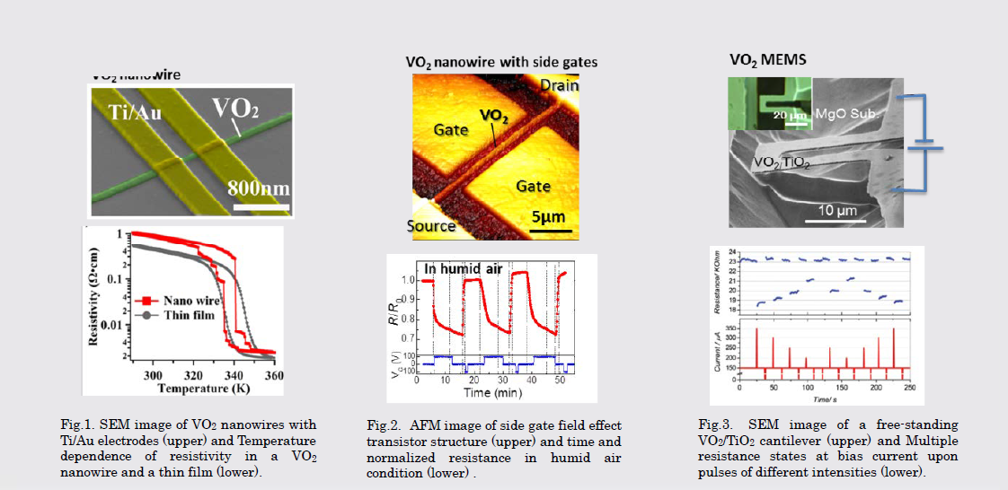
研究図Research Figure
文献 / Publications
Appl. Phys. Lett. 104, 023104 (2014), Phys. Rev B 89, 035141 (2014), Appl. Phys. Exp. 7, 045201 (2014). Adv. Mater. 25, 6430 (2013).,
Appl. Phys. Lett. 102, 0153106 (2013). Adv. Mater. 24, 2929 (2012)
研究者HP
- kanki
 sanken.osaka-u.ac.jp
 - http://www.sanken.osaka-u.ac.jp/labs/bis/