
IMRAM
Institute of Multidisciplinary Research for Advanced Materials, Tohoku University
東北大学
多元物質科学研究所

LAST UPDATE 2021/05/06
-
研究者氏名
Researcher Name森川大輔 Daisuke MORIKAWA
助教 Assistant Professor -
所属
Affiliation東北大学 多元物質科学研究所
計測研究部門 ナノ電子プローブ回折計測研究分野
Institute of Multidisciplinary Research for Advanced Materials, Tohoku University
Division of Measurements, Nano-Electron Probe Diffractometry -
研究キーワード
Research Keywords電子顕微鏡法
収束電子回折法
結晶構造解析
Transmission electron microscopy
Convergent-beam electron diffraction
Crystal structure analysis
- 研究テーマ
Research Subject -
収束電子回折法を用いた局所構造解析手法の開発と界面やその場観察への応用
Local structure analysis applied for interface and in-situ experiment using convergent-beam electron diffraction
研究の背景 Background of the Research
透過型電子顕微鏡(TEM)はナノメータスケールの微小領域の解析が可能な強力な装置です.また電子回折実験では,レンズによる収差の影響がほぼないことから,従来のイメージングによる分解能を越える解析が可能です.特に収束電子回折法は,電子線の多重散乱の効果をフルに活用することで,ほとんどの空間群を一意に決定できる他,価電子分布に敏感な静電ポテンシャル分布を直接決定できることから,わずかな電子雲のズレや結合などの検出が可能であると期待されています.
Transmission electron microscopy (TEM) is a powerful tool for an analysis in nano-scale specimen areas. Electron diffraction using a TEM is not almost affected by aberrations come from lens system. Thus, it is possible to achieve higher resolution than conventional imaging techniques. Especially, convergent-beam electron diffraction (CBED) can determine almost all crystal space group uniquely using dynamical scattering effect. CBED can be also used for a determination of electrostatic potential which is sensitive for slight deviation on electron density and bonding state at valence electrons.
研究の目標 Research Objective
電子顕微鏡のマイクロスコピー機能との併用により,ナノメータスケールでの精密構造解析を目指します.特に結晶界面やドメイン壁等の局所領域の解析[1,2]に有用で,分極ナノドメインの電圧印加その場観察[3]も可能です.現在,第一原理計算との組み合わせによる新しい局所領域構造解析,物性解析手法の開発[4,5]に取り組んでいます.さらに機械学習を応用した2次元的な結晶情報のマッピングや,ソフトマテリアルへの応用にも挑戦してまいります.
By using a combination with microscopy in TEM, we develop an accurate crystal structure analysis method for nano-scale specimen area. CBED method is a very powerful and useful technique for analysis in interfaces of crystal [1], domain boundaries [2] and in-situ observation of polar nano domains under electric field [3]. We are also trying a development of new technique with a combination of CBED and first principal calculation [4,5]. Two-dimensional mapping of crystal information with using machine-learning and applications for soft materials are also future targets.
研究図Figures
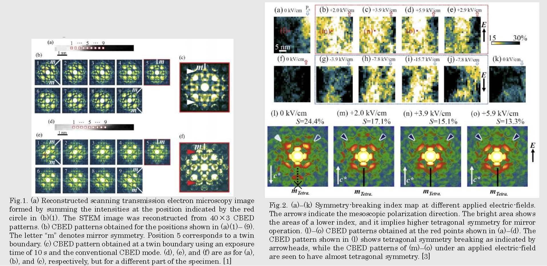
Fig.2. (a)–(k) Symmetry-breaking index map at different applied electric-fields. The arrows indicate the mesoscopic polarization direction. The bright area shows the areas of a lower index, and it implies higher tetragonal symmetry for mirror operation. (l)–(o) CBED patterns obtained at the red points shown in (a)–(d). The CBED pattern shown in (l) shows tetragonal symmetry breaking as indicated by arrowheads, while the CBED patterns of (m)–(o) under an applied electric-field are seen to have almost tetragonal symmetry. [3]
論文発表 / Publications
[1] D. Morikawa and K. Tsuda, Appl. Phys. Lett. 118, 092901 (2021).
[2] D. Morikawa, Y. Noguchi, and K. Tsuda, Jpn. J. Appl. Phys., 62, SM1003 (2023).
[3] D. Morikawa and K. Tsuda, Appl. Phys. Lett. 119, 052904 (2021).
[4] Md S. Islam, D. Morikawa et al., Phys. Rev. B 105, 174114 (2022).
[5] Md S. Islam, D. Morikawa et al., Phys. Rev. B 108, L060104 (2023).
研究者連絡先 / HP
- daisuke.morikawa.e5
 tohoku.ac.jp
 - https://www2.tagen.tohoku.ac.jp/lab/tsuda/