
IMCE
Institute for Materials Chemistry and Engineering, Kyushu University
九州大学
先導物質化学研究所
LAST UPDATE 2020/06/09
-
研究者氏名
Researcher Name斉藤光 Hikaru SAITO
准教授 Associate Professor -
所属
Affiliation九州大学 先導物質化学研究所
融合材料部門
Institute for Materials Chemistry and Engineering, Kyushu University
Department of Integrated Materials -
研究キーワード
Research Keywordsナノフォトニクス
電子顕微鏡
電子線分光
Nanophotonics
Electron microscopy
Electron beam spectroscopy
- 研究テーマ
Research Subject -
電子線励起光学現象の研究と新たなナノ顕微分光法の開発
Study on nanophotonic phenomena excited by an electron beam and development of new nano-spectroscopy method
研究の背景 Background of the Research
電子顕微鏡は原子分解能で物質・材料を可視化する究極の解析ツールとして知られていますが、電子線と試料の相互作用の結果生じる電子線の非弾性散乱や試料からの発光を通じて励起状態を分光学的に解析することもできます。この電子線分光の最大の魅力は電子顕微鏡の高い空間分解能を活用できる点にありますが、近年次々と発見されている電子線励起特有の現象をさらに活用すれば、動的観察や電子線損傷を抑えたソフトマテリアルの観察の実現に繋がると期待されています。
Electron microscopes are known as the ultimate analytical tool for visualizing materials at an atomic resolution. Furthermore, the excited states can be spectroscopically analyzed by inelastic electron scattering resulting from interaction between the electron beam and samples or light emission from the samples. Recently variety phenomena unique to electron beam excitation have been discovered due to rapid advancement of electron microscopy and spectroscopy, which are expected to generate new microspectroscopies as well as ultrafast dynamic observation and damage-less observation.
研究の目標 Research Objective
金属表面に励起される表面プラズモンを利用した物質の光吸収や発光の増強、新機能の付加を試みています。電子線分光により増強された光―物質相互作用の詳細をナノレベルで可視化することができるようになってきました。さらに、新規な電子線特有の物質との相互作用が見つかってきており、これを積極的に利用した新たな手法や電子顕微鏡周辺デバイスの開発を通して、励起と緩和過程のダイナミクスにまで踏み込んだ解析の実現を目指しています。
I am trying to enhance or manipulate light absorption and emission of materials using surface plasmons excited on the metal surface. It has become possible to visualize the details of light-matter interaction by electron beam spectroscopy at a nano scale. Furthermore, new electron beam-material interactions have been discovered. Through the development of electron microscope-related devices, I am aiming to establish new analysis method revealing dynamics of excitation and relaxation processes.
研究図Figures
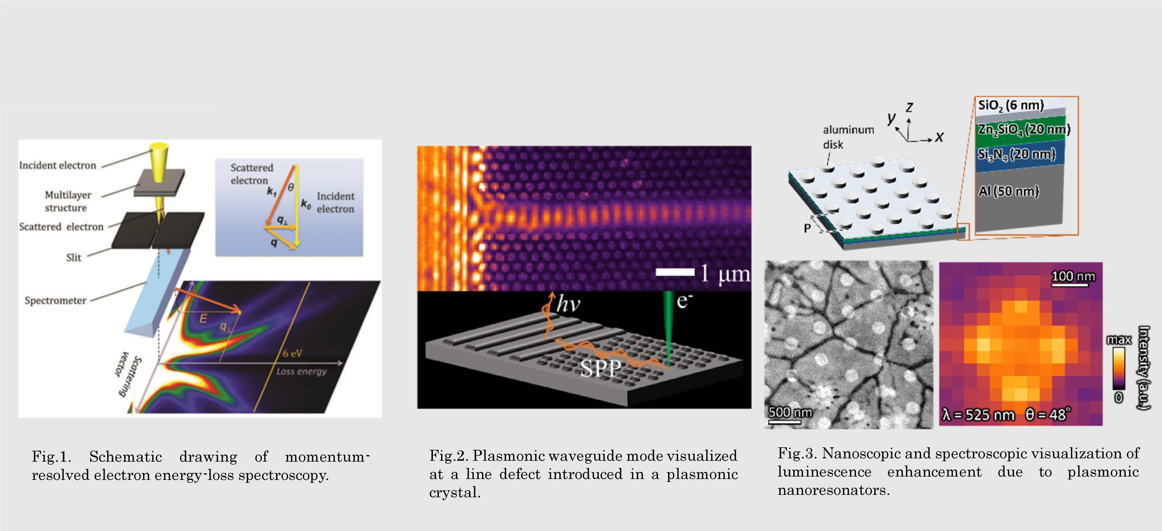
Fig.2. Plasmonic waveguide mode visualized at a line defect introduced in a plasmonic crystal.
Fig.3. Nanoscopic and spectroscopic visualization of luminescence enhancement due to plasmonic nanoresonators.
論文発表 / Publications
Microscopy 63, 85 (2014). Opt. Express 23, 2524 (2015). J. Appl. Phys. 117, 133107 (2015). Nano Lett. 15, 6789 (2015). Nano Lett. 15, 5764 (2015).
Light : Sci. Appl. 5, e16146 (2016). ACS Photon. 4, 1361 (2017). ACS Photon. 5, 4476 (2018). ACS Photon. 6, 2618 (2019). Phys. Rev. B 100, 242502 (2019).
研究者連絡先 / HP
- Saito.hikaru.961
 m.kyushu-u.ac.jp
 - https://hyoka.ofc.kyushu-u.ac.jp/search/details/K005792/index.html