IMRAM
Institute of Multidisciplinary Research for Advanced Materials, Tohoku University
東北大学
多元物質科学研究所
LAST UPDATE 2021/05/06
-
研究者氏名
Researcher Name佐藤庸平 Yohei SATO
准教授 Associate Professor -
所属
Professional Affiliation東北大学多元物質科学研究所
計測研究部門 電子回折・分光計測研究分野
Institute of Multidisciplinary Research for Advanced Materials, Tohoku University
Division of Measurements, Electron-Crystallography and-Spectroscopy -
研究キーワード
Research Keywords電子エネルギー損失分光法
電子顕微鏡法
ナノ材料物性解析
Electron energy-loss spectroscopy
Transmission electron microscopy
Analysis for optical/dielectric properties of nano-scale materials
- 研究テーマ
Research Subject -
電子ナノプローブを用いたナノマテリアルの誘電特性解析
Analysis for dielectric properties of nano-scale materials using nm electron probe
研究の背景 Background
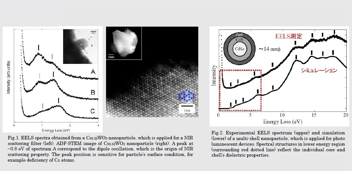
透過型電子顕微鏡(TEM)を用いた電子エネルギー損失分光法(EELS)は、ナノスケール局所領域から材料の光学・誘電的特性や非占有状態の電子構造を明らかにします。この手法を用いることで、ナノ粒子・ナノワイヤーなどのナノマテリアルや不純物などを多く含む機能性材料の単相領域からの分光測定を行うことが可能です。
Electron energy-loss spectroscopy (EELS) based on transmission electron microscopy (TEM) reveals the optical/dielectronic properties and the unoccupied electronic states of materials. This analytical technique enables to reveal optical/dielectric properties of individual nanomaterials or single phase area of new functional materials including impurities.
研究の目標 Outcome
機能性ナノ粒子はバルク試料とは異なる誘電的・光学的性質を持ち、光学散乱フィルター・高効率発光材として応用されています。更なる機能性向上に向けた材料開発のために、ナノ粒子1粒1粒からTEM-EELS測定を行い、光学特性や電子構造の起源を解明することを目指します。
The functional nano-particles, which have various optical properties different from bulk materials, are applied for optical scattering filters and high efficient luminescence materials, etc. We research origins of the characteristic properties or electronic structures of the functional nanoparticles by conducting TEM-EELS measurements for the purpose of developing the materials improved such functions.
研究図Research Figure
文献 / Publications
Microsc. Microanal. 20 (2014) 807–814., J. Phys. Conf. Ser. 500 (2014) 192013, J. Appl. Phys. 112 (2012) 074308, Diamond & Related Materials, 25 (2012) 40–44, Ultramicroscopy, 111 (2011) 1381–1387.
研究者HP
- yohei.sato.c4
 tohoku.ac.jp
 - http://www.tagen.tohoku.ac.jp/labo/terauchi/index.html