SANKEN
The University of Osaka
大阪大学
産業科学研究所
LAST UPDATE 2017/02/26
-
研究者氏名
Researcher Name田中秀和 Hidekazu TANAKA
教授 Professor -
所属
Affiliation大阪大学 産業科学研究所
産業科学ナノテクノロジーセンター
SANKEN, The University of Osaka
Nanoscience and Nanotechnology Center, -
研究キーワード
Research Keywords機能性酸化物
ナノ材料・デバイス
ナノ新物性探索
Functional oxide materials
Nano-materials and Nano-devices
Nano -material and physics
- 研究テーマ
Research Subject -
機能性酸化物ナノエレクトロニクスの構築
Functional oxide nanoelectrnocs
研究の背景 Background of the Research
機能性酸化物を始めとするSiに無い機能を有するエキゾティクマテリアルに対し、ボトムアップナノテクノロジーの1つである原子・分子層制御人工格子形成技術を駆使し、空間的、エネルギーレベル的に最適な配置・組み合わせを考慮した原子・分子配列を有するナノ機能材料を創製します。量子効果が支配的となるナノスケールにおいて物質の性質を設計することにより、従来に無い、あるいは凌駕する機能を創出し、従来の原理を超えた機能を発現するマテリアル・デバイスの創出を行います。
The main purpose of this department is to newly construct function harmonized nano-materials and nano-devices based on novel nano-scale physical mechanism. By using typical "Bottom-up Nanotechnology" of artificial lattice technique , we combine exotic materials which exhibit ferroelectric/ferromagnetic/semiconductive properties and so on at atomic/molecular level to new functional nanomaterials. We also develop nano-fabrication technique for the new functional nano-materials by fusion of Bottom-up and Top-down Nanotechnologies, and construct spatially and dimensionally controlled nanodevices toward new functional electronics application.
研究の目標 Research Objective
機能性酸化物は僅かな外場で金属-絶縁体相転移に伴う巨大抵抗変化を示す魅力的な物質であり、sub-10nmスケールまで巨大相転移動作を発現し、将来の低消費電力・高速・極微細デバイスの創出が期待されているが、その挙動は未だ明らではありません。原子・分子配列を直接的に制御するボトムアップ手法(パルスレーザ蒸着薄膜結晶成長)とトップダウン手法(ナノリソグラフィー)に融合により、異なる機能を持つ酸化物を組み合わせる「ヘテロ構造」、格段に小さな「ナノヘテロ構造」を創出し、新機能スピンエレクトロニクスデバイス、省・創エネルギーデバイスを創出します。
Transition metal oxides exhibit a rich variety of attractive properties such as a metal-insulator transition (MIT), colossal magnetoresistance, and High TC ferromagnetism due to their strongly correlated electrons. We produce novel electronics devices to control their MIT and ferromagnetism in 3D nanostructures and heterostrcutures toward functional oxide nanoelectronics and spintronics.
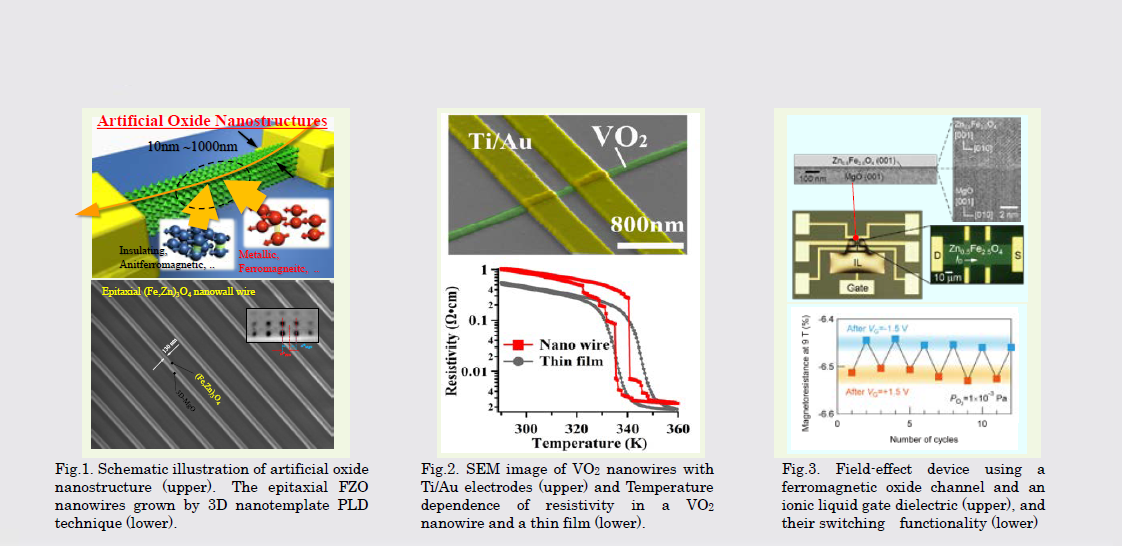
研究図Figures
論文発表 / Publications
Sci. Rep. 4 (2014) 5818, Adv. Materials Interfaces 1 (2014) 1300108, Appl. Phys. Lett. 104 (2014) 023104, Appl. Phys. Lett. 105 (2014) 023502., Phys. Rev. B 90 (2014) 054203, Phys.
Rev. B 89 (2014) 035141, Appl. Phys. Exp. 7 (2014)045201, Adv. Materials 25 (2013) 6430, Appl. Phys. Lett. 102 (2013) 153106, Appl. Phys. Lett. 103 (2013) 223105
研究者連絡先 / HP
- h-tanaka
 sanken.osaka-u.ac.jp
 - http://www.sanken.osaka-u.ac.jp/labs/bis/