
IMRAM
Institute of Multidisciplinary Research for Advanced Materials, Tohoku University
東北大学
多元物質科学研究所

LAST UPDATE 2021/05/08
-
研究者氏名
Researcher Name中川勝 Masaru NAKAGAWA
教授 Professor -
所属
Affiliation東北大学 多元物質科学研究所
マテリアル・計測ハイブリッド研究センター
Institute of Multidisciplinary Research for Advanced Materials, Tohoku University
光機能材料化学分野
Materials-Measurement Hybrid Research Center,
Photo-Functional Material Chemistry -
研究キーワード
Research Keywords超微細加工レジスト材料
超精密位置合わせ・積層プロセス
人工反応場
Resist materials for super fine patterning
Process for super fine overlay and integration process
Meta-site
- 研究テーマ
Research Subject -
省エネ型ナノ加工のナノインプリント技術で,革新的光学素子や化学反応場の構築
Creation of innovative meta-optics and meta-sites by nanoimprint fabrication technology
研究の背景 Background of the Research
成形加工サイズが一桁ナノメートルに近づくにつれ、分子との相関が強く現れてきます。電子線描画を用いる電子線リソグラフィや有型成形加工技術の光ナノインプリントリソグラフィ(UV-NIL)では、一桁ナノサイズからのパターン成形や転写が求められています。特にUN-NILは、半導体デバイスや3次元ナノ構造オプティクス(メタオプティクス)などで産業化が進んでおり、レジスト材料の化学とプロセス加工の物理が益々必要とされ、デバイス創出に向けた設計・集積化技術の革新が求められています。
As the forming process size approaches single-digit nanometers, the correlation with molecules becomes stronger. In electron beam lithography based on electron beam drawing and ultraviolet nanoimprint lithography (UV-NIL) based on molding and processing technology, pattern molding and transfer at more than single-digit nanometer sizes are required. UN-NIL, in particular, is being industrialized in semiconductor devices and 3D nanostructure optics (meta-optics), which increasingly require the chemistry of resist materials and the physics of process processing, and innovation in design and integration technology for device creation.
研究の目標 Research Objective
UV-NILのモールド製造に資する電子線レジスト高分子材料や光硬化レジスト分子材料の開発をゼプトモルの化学の観点から切り開きます。超精密な基板配置を可能にするレーザー加工孔版印刷を特徴とする新しい成形加工プロセス、重ね合わせや積層に資する原子精度や1桁ナノ精度の位置合わせを行う光計測や積層の学術を構築します。金属や誘電体の3次元ナノ構造体が発現する革新的な化学反応を誘起する人工反応場(メタサイト)の概念の実証を目指します。
Our research will open the development of electron-beam resist polymer materials and photo-curable resist molecular materials that contribute to the production of UV-NIL molds and devices from the perspective of “zepto-mole chemistry”. We will build new molding and fabrication processes featuring laser-drilled screen printing that enable ultra-precise substrate placement, and optical metrology and stacking science for atomic- and single-digit-nanometer-accuracy positioning that is conducive to overlay and stacking. We will demonstrate the concept of artificial reaction fields (meta-sites) that induce innovative chemical reactions exhibited by metallic and dielectric 3D nanostructures.
研究図Figures
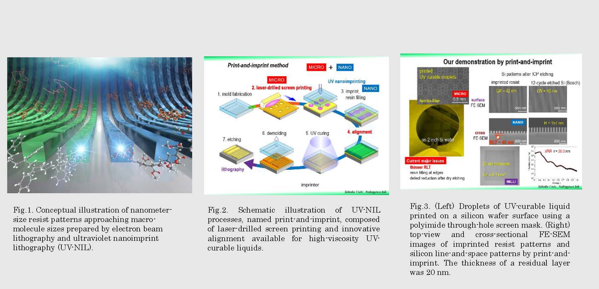
Fig.2. Schematic illustration of UV-NIL processes, named print-and-imprint, composed of laser-drilled screen printing and innovative alignment available for high-viscosity UV-curable liquids.
Fig.3. (Left) Droplets of UV-curable liquid printed on a silicon wafer surface using a polyimide through-hole screen mask. (Right) top-view and cross-sectional FE-SEM images of imprinted resist patterns and silicon line-and-space patterns by print-and-imprint. The thickness of a residual layer was 20 nm.
論文発表 / Publications
J. Phys. Chem. C, 128(12), 5271 (2024). Jpn. J. Appl. Phys., 63, 04SP04 (2024). J. Vac. Sci. Technol. B, 40, 062602 (2022). [Review] Jpn. J. Appl. Phys., 61, SD0805 (2022). Chem. Lett., 50, 1403 (2021). Sci. Rep., 11, 16550 (2021). ACS Appl. Mater. Interfaces, 9, 6591 (2017).
研究者連絡先 / HP
- masaru.nakagawa.c5
 tohoku.ac.jp
 - https://researchmap.jp/read0143910
- http://www2.tagen.tohoku.ac.jp/lab/nakagawa/(研究室HP)